Charge Density in Semiconductor
Carrier Concentration in N-type Semiconductor Consider Nd is the donor Concentration ie the number of donor atoms per unit volume of the material and Ed is the donor energy level. This is the strong inversion case in which we have a significant conducting sheet of inversion charge at the interface.

Charge Density An Overview Sciencedirect Topics
The journal publishes cutting-edge research on the physical properties of semiconductors and their applications.
. In physics a charge carrier is a particle or quasiparticle that is free to move carrying an electric charge especially the particles that carry electric charges in electrical conductors. In a conducting medium an electric field can exert force on these free particles causing a net motion of the. Sign up for new issue notifications Current volume Number 10 October 2022 Number 9.
Lateral polarization GaN HEMTs. Suppose we have taken one conductor of cross-section 25 square mm. Now the electric current carried by the conductor per square mm of its cross.
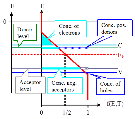
Thus accommodating more electrons. Charge density in the depletion regions is then due to the ionized donors and acceptors and is as shown below. In 100 million parts of semiconductor one part of impurity is added.
Providing optical and charge-carrier confinement. Using the density matrix theory of semiconductor lasers with relaxation broadening Asada et al. The net charge on both sides of the junction has to be equal and opposite qNd xn qNaxp 0 elsewhere 0 0 qN x x qN x x x a p d n Knowing the charge density one can calculate the electric field and the potential drops using Gausss law.
As per theory of semiconductor impure semiconductors are called extrinsic semiconductors. N-type and P-type semiconductors. Researchers based in China and Saudi Arabia propose lateral modulation of the charge polarization of III-nitride material as a more effective route to electrically isolate high-electron-mobility transistors compared with mesa etching or ion implantation Yijun Dai et al Appl.
The charge output of the TENGs can be increased by enhancing tribo-materials surface charge density 18192021. The symbol ψ is used to signify the potential in the semiconductor measured relative to the potential at a position x deep inside the semiconductor. The gain and hence the laser emission occurs at the direct bandgap of the active layer at wavelengths in the range.
Depending on the type of impurity added we have two types of semiconductors. The concept of current density is very simple but it is much use full in the field of electrical engineering. For electrons the current density J amperes per meter squared is written.
Extrinsic semiconductor is formed by adding a small amount of impurity. First proposed by Clement D. Child in 1911 Childs law states that the space-charge-limited current SCLC in a plane-parallel vacuum diode varies directly as the three-halves power of the anode voltage and inversely as the square of the distance d separating the cathode and the anode.
In a p-type semiconductor there is an increase in the density of unfilled states. Metal oxide semiconductors have gained attention in monitoring and deducting explodes and harmful gases due to their optical electrical and thermal properties. Submit an article opens in new tab Track my article opens in new tab.
Semiconductor Science and Technology is IOPs journal dedicated to semiconductor research. Tribovoltaic effect on metalsemiconductor interface for direct. Note that ψ becomes positive.
With increase of temperature more and more donor atoms get ionized and the density of electrons in the. When the temperature rises above absolute zero these charge carriers will begin to occupy states above Fermi level. The charge species shows a rise concomitant with the fast initial decay of the singlet species.
When we apply the external voltage across the semiconductor diode in such a way that the positive terminal of the battery is connected to its n-side and the negative terminal of the battery is connected to the p-side of the diode then it is said to be in the condition of reverse biasWhen an external voltage is applied across the diode as the direction of the external voltage is the same. Current Density in Metal. Examples are electrons ions and holesThe term is used most commonly in solid state physics.
At very low temperatures all donor levels are filled with electrons. They are highly sensitive and have a short response time when fabricated at the nanoscale Chatterjee et al 2015The most common metal oxide semiconductor materials that found application as sensors are SnO 2. Concentration at the interface exceeds the doping density in the semiconductor.
Microelectronics 28 July 2022. In all cases the material is epitaxially grown meaning that the entire laser chip forms a single crystal. 550 nm 200 fs pump pulse excitation density 10 18 excitationscm 3.
Now due to applied electric potential the conductor carries a current of 3 A. The charge carriers in this state have their own quantum states and generally do not interact with each other.

Advanced Texts In Physics Semiconductor Physics An Introduction Edition 9 Hardcover Walmart Com Semiconductor Physics Physics Semiconductor

Charge Density Wave An Overview Sciencedirect Topics

Current Density In Metal And Semiconductor Electrical4u
2 2 2 Doping And Carrier Density
No comments for "Charge Density in Semiconductor"
Post a Comment